Hardware Schematics
Exposed pads
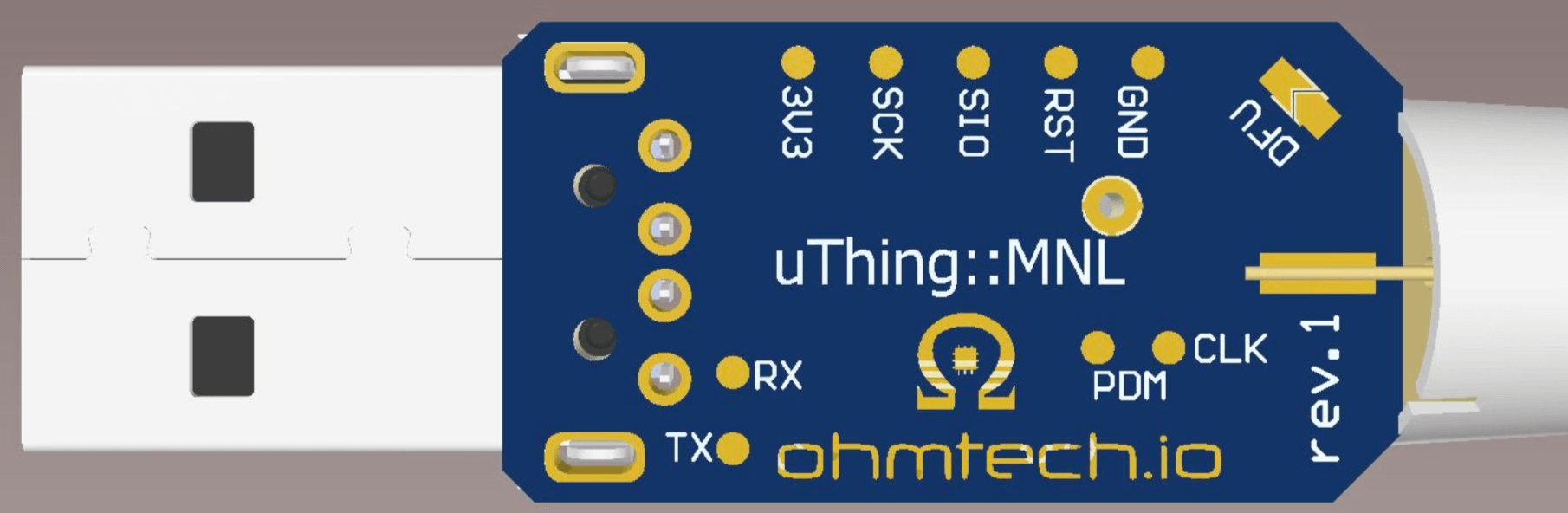
The table below details the connection of the exposed pads:
| ID | Pin # | Signal name | Comment |
|---|---|---|---|
| TX | 8 | PA.2 | USART2_TX (UART TXD MCU side, connect to RXD in a transceiver or MCU) |
| RX | 9 | PA.3 | USART2_RX (UART RXD, connect to TXD) |
| PDM | 12 | PA.6 | SPI1_MISO used to receive Mic PDM data |
| CLK | 11 | PA.5 | SPI1_CLK used as PDM clock signal |
| DFU | 31 | PB.8 | BOOT0 (short this pad to boot the MCU in USB DFU mode) |
| GND | 16,32 | GND | System reference ground |
| 3V3 | 1,17 | VDD | Regulated 3.3V rail (150mA max.) |
| SCK | 24 | PA.14 | SWD Clock signal |
| SIO | 23 | VDD | SWD Data signal |
| RST | 4 | NRST | Reset signal |
Circuit Schematic
uThing::MNL revision 1 schematic:
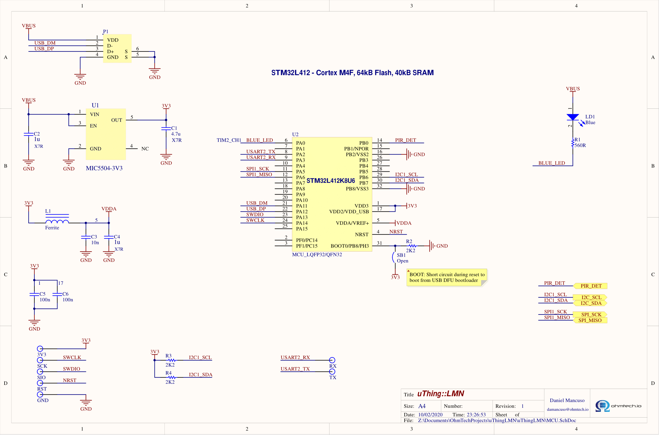
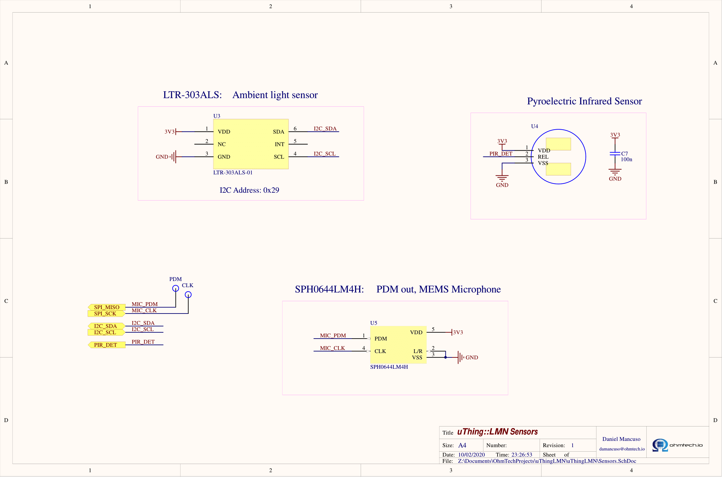
(PDF version here)